
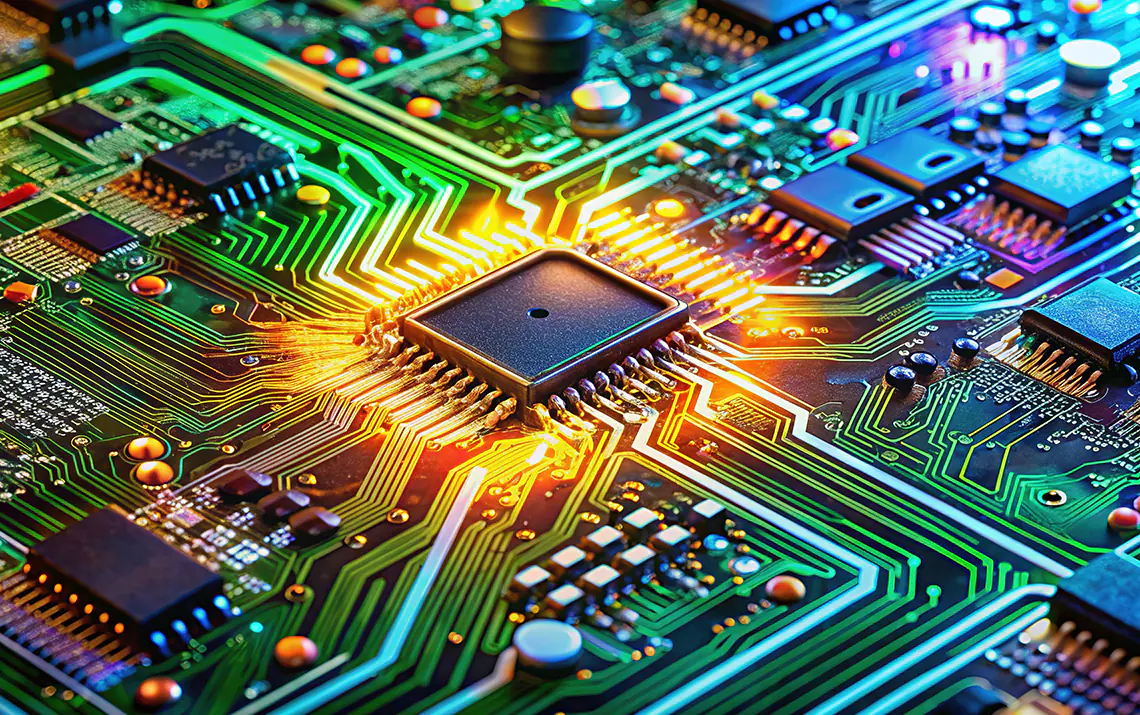
In today’s ultra-competitive electronics manufacturing landscape—from smartphones to medical devices—the Printed Circuit Board (PCB) is the silent hero. Yet as these boards grow denser and more complex, detecting tiny, critical defects becomes increasingly challenging. That’s where Intelgic steps in with their next-gen PCB Board Inspection technology, merging machine vision systems, micron-level defect detection, and robotic imaging systems for a revolutionary inspection process.
The Inspection Imperative for Modern PCBs
PCBs now host vast arrays of micro-components—SMDs, BGAs, resistors, capacitors—stacked across multiple depths and miniaturized geometries. Manual or rudimentary optical inspection simply can’t scale to catch subtle issues like misplacements, solder irregularities, or microscopic substrate damage.
- Complex multi-layer boards with hundreds of tiny parts
- Depth variation ranging from flat substrates to tall components
- Critical space for defects such as solder bridges, lifted pins, or substrate scratches at the micron level
Intelgic’s Automated PCB Inspection Solution
Intelgic addresses these challenges with a comprehensive system that pairs machine vision and AI with precision robotics:
Multi-Focus Vision and Microscopic Imaging
Using high-resolution cameras and telecentric lenses, the system performs multi-focus imaging, capturing stacked visuals at different focal points across the board’s Z-axis. These are then stitched into one ultra-clear, deep-of-field image.
Precise Component Detection and Verification
AI algorithms detect and categorize components—recognizing SMD types, reading serial labels, and confirming accurate orientation and placement vs. BOM/CAD models. Missing, extra, or misaligned parts trigger real-time alerts.
Micron-Level Defect Detection
Thanks to ultra-high-resolution imaging and advanced AI analytics, defects as small as a few microns—like solder bridges, cold joints, tombstoning, or substrate scratches—are reliably detected.
Robotic Imaging Systems
Intelgic’s 3-axis robotic rail platform moves the camera and lighting smoothly across X, Y, and Z axes. This enables totally consistent imaging even for large or irregularly shaped PCBs. Height is adjusted in real time to cope with component variation.
Dynamic Lighting and Real-Time Reporting
Adaptable lighting modules—coaxial, ring, or dome—track with the camera to maintain consistent illumination. AI-inspection results are generated in real time, integrated with MES systems, and logged with full traceability.
Advantages of Advanced AI-Based PCB Inspection
| Benefit | Impact |
| Unparalleled Accuracy | Detects sub-micron defects beyond human vision |
| High Throughput | Robots enable rapid, repeatable inspections |
| Flexible Component Coverage | Works across board types and layouts |
| Robust Traceability | Detailed logs and audit trails help QA and compliance |
| Adaptive Intelligence | AI improves with each inspection, reducing false rates |
Real-World Use Cases
Consumer Electronics
In smartphones and tablets with ultra-dense boards, this system prevents errors like misplaced 0201 capacitors and microscopic solder flaws—boosting first-pass yield and reliability.
Automotive Systems
ECUs and BMS boards demand flawless soldering. Robotic AOI ensures defect-free builds by inspecting high-density PCBs with precision, spot-checking lifted pins or cold joints.
Medical Devices
Insulin pumps, diagnostic equipment, and implantable PCBs require microscopic inspection for coating flaws, solder debris, and labeling accuracy. AI-powered AOI brings unmatched consistency.
Aerospace & Industrial Controls
PCBs in avionics or industrial robots need to function flawlessly over years. Micron-level inspections ensure the reliability required in mission-critical environments.
How Intelgic Outclasses Traditional Inspection
- Multi-depth Imaging eliminates focus issues caused by varying component heights
- Robotic Accuracy removes human error and stress from precision inspection
- AI Intelligence steps beyond rule-based detection, enabling smarter, adaptive inspection models
- Data Analytics via Intelgic’s Live Vision turns test results into continuous improvement with heatmaps, trend tracking, and cross-line comparisons
Integration Blueprint: From Setup to Insight
- Configure Robotics & Optics
Set Z-range, lighting, and scan paths based on board complexity. - Capture Multi-Focus Data
Traverse boards with mosaic photographing for full coverage. - AI-Driven Detection
Automatically identify placement issues, missing elements, and defects. - Automate Reporting
Export pass/fail logs, annotated boards, and key metrics to MES. - Iterate and Improve
Use analytical feedback to refine inspection thresholds and defect targeting.
The Road Ahead for PCB Inspection
- Ensemble AI Models combining YOLO, EfficientDet, and others to enhance defect detection accuracy
- GAN-Augmented Learning to teach AI rare or complex PCB defects
- Edge Processing for ultra-low latency and immediate on-line decision-makin.
- Augmented Reality Feedback overlaying inspection results for operator validation
Intelgic’s sophisticated PCB Board Inspection solution, empowered by micron-level defect detection and robotic imaging systems, is redefining quality control in electronics manufacturing. It enables manufacturers to catch the minutest flaws at scale, secure manufacturing integrity, and drive smarter production from first assembly to final QA.
For companies that demand zero defect, precision accuracy, and streamlined workflow, this is more than tech—it’s the future of inspection.